Mudanças entre as edições de "Níveis lógicos"
Ir para navegação
Ir para pesquisar
Figura 1 - Níveis e chaveamento digital
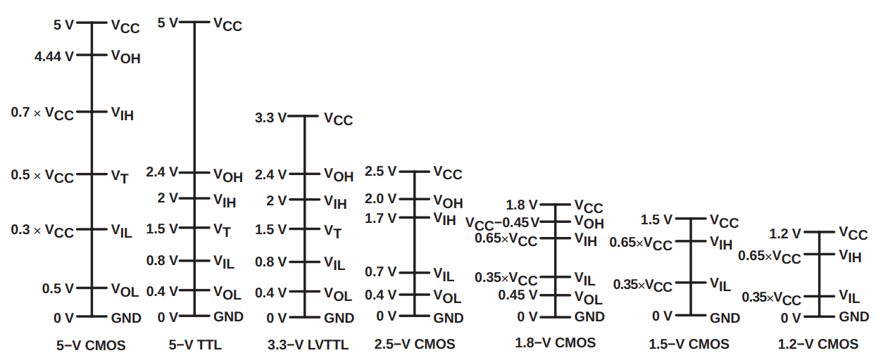
Fonte: Selecting the Right Level-Translation Solution - TI.
Quadro 1 - I/O Standards Support for FPGA I/O in Intel® Arria® 10 Devices
FONTE: Intel® Arria® 10 Core Fabric and General Purpose I/Os Handbook
| (3 revisões intermediárias pelo mesmo usuário não estão sendo mostradas) | |||
| Linha 2: | Linha 2: | ||
{{fig|1|Níveis e chaveamento digital | LogicSwitching.png| 1200 px | [https://www.ti.com/lit/an/scea035a/scea035a.pdf Selecting the Right Level-Translation Solution - TI]}} | {{fig|1|Níveis e chaveamento digital | LogicSwitching.png| 1200 px | [https://www.ti.com/lit/an/scea035a/scea035a.pdf Selecting the Right Level-Translation Solution - TI]}} | ||
| − | <center> Quadro 1 - I/O Standards Support for FPGA I/O in Intel® Arria® 10 Devices | + | <center> Quadro 1 - I/O Standards Support for FPGA I/O in Intel® Arria® 10 Devices |
{| class="wikitable" style="text-align:center;" | {| class="wikitable" style="text-align:center;" | ||
|- style="font-weight:bold; background-color:#c0c0c0; color:#333;" | |- style="font-weight:bold; background-color:#c0c0c0; color:#333;" | ||
| Linha 231: | Linha 231: | ||
| — | | — | ||
|} | |} | ||
| − | + | FONTE: [https://www.intel.com/content/www/us/en/docs/programmable/683461/current/i-o-standards-support-for-fpga-i-o-in.html Intel® Arria® 10 Core Fabric and General Purpose I/Os Handbook] </center> | |
| − | + | Ler mais em | |
| + | *[https://www.intel.com/programmable/technical-pdfs/654427.pdf Selectable I/O Standards in Stratix & Stratix GX Devices] | ||
| + | *[https://onlinedocs.microchip.com/pr/GUID-53092BEF-DCEB-4741-9EFC-5843AA55C657-en-US-1/index.html?GUID-B4434174-E143-4711-BDD8-A67451768D1C#GUID-B4434174-E143-4711-BDD8-A67451768D1C__ID-00001D8D Supported I/O Standards Microchip] | ||
<!-- | <!-- | ||
:[[Arquivo:TI_CMOS_Voltage_vs_Speed.png]] | :[[Arquivo:TI_CMOS_Voltage_vs_Speed.png]] | ||
| Linha 242: | Linha 244: | ||
*[http://digsys.upc.es/csd/units/Elect/TI_Digital_Logic_Families.pdf Digital Logic Family Selection Matrix (Sorted by Speed)] | *[http://digsys.upc.es/csd/units/Elect/TI_Digital_Logic_Families.pdf Digital Logic Family Selection Matrix (Sorted by Speed)] | ||
--> | --> | ||
| + | |||
| + | ==O que fazer quando se trabalha com diferentes tensões lógicas?== | ||
| + | *Uma das possíveis soluções é usar circuitos apropriados para translação das tensões. Um excelente guia para isso é o [https://www.ti.com/logic-voltage-translation/voltage-translators-level-shifters/overview.html Voltage translators & level shifters] da Texas Instruments. Alguns exemplos são mostrados no ''Application Report'' [https://www.ti.com/lit/an/scea030b/scea030b.pdf?ts=1695878113649Voltage Translation Between 3.3-V, 2.5-V, 1.8-V, and 1.5-V Logic Standards]. | ||
| + | *Um exemplo é o ''Application Report'' [https://www.ti.com/lit/an/slva675b/slva675b.pdf?ts=1695932316421 Voltage-Level Translation With the LSF Family]. Sua aplicação para tensão de entrada de 1.8V e saída de 3.3V é ilustrada na simulação no [https://tinyurl.com/23ga4s7m FALSTAD]. | ||
| + | :[[Arquivo:FALSTAD_SLVA675B.png | 1000px]] | ||
==O que é a margem de ruído?== | ==O que é a margem de ruído?== | ||
Edição atual tal como às 18h13min de 28 de setembro de 2023
Quais são as famílias lógicas dos circuitos digitais?
Figura 1 - Níveis e chaveamento digital

| I/O Standard | Device Variant Support | I/O Buffer Type Support | Application | Standard Support | |
|---|---|---|---|---|---|
| LVDS I/O | 3V I/O | ||||
| 3.0 V LVTTL/3.0 V LVCMOS | Devices with 3 V I/O banks only. | No | Yes | General purpose | JESD8-B |
| 2.5 V LVCMOS | Devices with 3 V I/O banks only. | No | Yes | General purpose | JESD8-5 |
| 1.8 V LVCMOS | All | Yes | Yes | General purpose | JESD8-7 |
| 1.5 V LVCMOS | All | Yes | Yes | General purpose | JESD8-11 |
| 1.2 V LVCMOS | All | Yes | Yes | General purpose | JESD8-12 |
| SSTL-18 Class I and Class II | All | Yes | Yes | DDR2 | JESD8-15 |
| SSTL-15 Class I and Class II | All | Yes | Yes | DDR3 | — |
| SSTL-15 | All | Yes | Yes | DDR3 | JESD79-3D |
| SSTL-135, SSTL-135 Class I and Class II | All | Yes | Yes | DDR3L | — |
| SSTL-125, SSTL-125 Class I and Class II | All | Yes | Yes | DDR3U | — |
| SSTL-12, SSTL-12 Class I and Class II | All | Yes | No | RLDRAM 3 | — |
| POD12 | All | Yes | No | DDR4 | JESD8-24 |
| 1.8 V HSTL Class I and Class II | All | Yes | Yes | DDR II+, QDR II+, and RLDRAM 2 | JESD8-6 |
| 1.5 V HSTL Class I and Class II | All | Yes | Yes | DDR II+, QDR II+, QDR II, and RLDRAM 2 | JESD8-6 |
| 1.2 V HSTL Class I and Class II | All | Yes | Yes | General purpose | JESD8-16A |
| HSUL-12 | All | Yes | Yes | LPDDR2 | — |
| Differential SSTL-18 Class I and Class II | All | Yes | Yes | DDR2 | JESD8-15 |
| Differential SSTL-15 Class I and Class II | All | Yes | Yes | DDR3 | — |
| Differential SSTL-15 | All | Yes | Yes | DDR3 | JESD79-3D |
| Differential SSTL-135, SSTL-135 Class I and Class II | All | Yes | Yes | DDR3L | — |
| Differential SSTL-125, SSTL-125 Class I and Class II | All | Yes | Yes | DDR3U | — |
| Differential SSTL-12, SSTL-12 Class I and Class II | All | Yes | No | RLDRAM 3 | — |
| Differential POD12 | All | Yes | No | DDR4 | JESD8-24 |
| Differential 1.8 V HSTL Class I and Class II | All | Yes | Yes | DDR II+, QDR II+, and RLDRAM 2 | JESD8-6 |
| Differential 1.5 V HSTL Class I and Class II | All | Yes | Yes | DDR II+, QDR II+, QDR II, and RLDRAM 2 | JESD8-6 |
| Differential 1.2 V HSTL Class I and Class II | All | Yes | Yes | General purpose | JESD8-16A |
| Differential HSUL-12 | All | Yes | Yes | LPDDR2 | — |
| LVDS | All | Yes | No | SGMII, SFI, and SPI | ANSI/TIA/EIA-644 |
| Mini-LVDS | All | Yes | No | SGMII, SFI, and SPI | — |
| RSDS | All | Yes | No | SGMII, SFI, and SPI | — |
| LVPECL | All | Yes | No | SGMII, SFI, and SPI | — |
Ler mais em
O que fazer quando se trabalha com diferentes tensões lógicas?
- Uma das possíveis soluções é usar circuitos apropriados para translação das tensões. Um excelente guia para isso é o Voltage translators & level shifters da Texas Instruments. Alguns exemplos são mostrados no Application Report Translation Between 3.3-V, 2.5-V, 1.8-V, and 1.5-V Logic Standards.
- Um exemplo é o Application Report Voltage-Level Translation With the LSF Family. Sua aplicação para tensão de entrada de 1.8V e saída de 3.3V é ilustrada na simulação no FALSTAD.

O que é a margem de ruído?

FONTE: How to Select Little Logic - Texas Instruments Incorporated
Obsolescência das famílias lógicas

FONTE: [1]
Encapsulamento de circuitos lógicos

FONTE: LOGIC MIGRATION GUIDE - Texas Instruments (TI)