Mudanças entre as edições de "Códigos VHDL para uso nas Aulas 2011-1"
| (12 revisões intermediárias por 2 usuários não estão sendo mostradas) | |||
| Linha 18: | Linha 18: | ||
</syntaxhighlight> | </syntaxhighlight> | ||
| − | + | ||
| − | < | + | == Descrição do hardware de um multiplexador de 4 para 1== |
| − | entity | + | |
| + | <syntaxhighlight lang=vhdl> | ||
| + | entity mux_novo is | ||
port | port | ||
( | ( | ||
-- Input ports | -- Input ports | ||
| − | + | X: in bit_vector (3 downto 0); | |
| + | S : in bit_vector (1 downto 0); | ||
-- Output ports | -- Output ports | ||
| − | C : out bit | + | Y : out bit |
| + | ); | ||
| + | end entity mux_novo; | ||
| + | |||
| + | -- Implementação com lógica pura | ||
| + | architecture Logica_pura of mux_novo is | ||
| + | |||
| + | begin | ||
| + | Y <= (X(0) and (not S(1)) and (not S(0))) or | ||
| + | (X(1) and (not S(1)) and (S(0))) or | ||
| + | (X(2) and (S(1)) and (not S(0))) or | ||
| + | (X(3) and (S(1)) and (S(0))); | ||
| + | end architecture Logica_pura; | ||
| + | |||
| + | -- Implementação com WHEN ELSE | ||
| + | architecture v_WHEN of mux_novo is | ||
| + | |||
| + | begin | ||
| + | Y <= X(0) when S = "00" else | ||
| + | X(1) when S = "01" else | ||
| + | X(2) when S = "10" else | ||
| + | X(3); | ||
| + | end architecture v_WHEN; | ||
| + | |||
| + | -- Implementação com WITH SELECT | ||
| + | architecture v_WITH_SELECT of mux_novo is | ||
| + | |||
| + | begin | ||
| + | with S select | ||
| + | Y <= X(0) when "00", -- note o uso da , | ||
| + | X(1) when "01", | ||
| + | X(2) when "10", | ||
| + | X(3) when others; -- note o uso de others, para todos os demais valores. | ||
| + | -- Não pode ser substituido por "11" mesmo que o signal seja bit_vector. | ||
| + | end architecture v_WITH_SELECT; | ||
| + | |||
| + | -- Implementação com IF ELSE | ||
| + | architecture v_IF_ELSE of mux_novo is | ||
| + | |||
| + | begin | ||
| + | |||
| + | |||
| + | end architecture v_IF_ELSET; | ||
| + | </syntaxhighlight> | ||
| + | |||
| + | <code> | ||
| + | vcom -93 -work work {/home/moecke/SST-2011-1/mux_41/mux_41.vhd} | ||
| + | vsim work.mux_41 | ||
| + | add wave \ | ||
| + | {sim:/mux_41/x } \ | ||
| + | {sim:/mux_41/s } \ | ||
| + | {sim:/mux_41/y } | ||
| + | |||
| + | # testando entrada 0 | ||
| + | force -freeze sim:/mux_41/s 00 0 | ||
| + | force -freeze sim:/mux_41/x 0001 0 | ||
| + | run | ||
| + | force -freeze sim:/mux_41/x 1110 0 | ||
| + | run | ||
| + | # testando entrada 1 | ||
| + | force -freeze sim:/mux_41/s 01 0 | ||
| + | force -freeze sim:/mux_41/x 0010 0 | ||
| + | run | ||
| + | force -freeze sim:/mux_41/x 1101 0 | ||
| + | run | ||
| + | # testando entrada 2 | ||
| + | force -freeze sim:/mux_41/s 10 0 | ||
| + | force -freeze sim:/mux_41/x 0100 0 | ||
| + | run | ||
| + | force -freeze sim:/mux_41/x 1011 0 | ||
| + | run | ||
| + | # testando entrada 3 | ||
| + | force -freeze sim:/mux_41/s 11 0 | ||
| + | force -freeze sim:/mux_41/x 1000 0 | ||
| + | run | ||
| + | force -freeze sim:/mux_41/x 0111 0 | ||
| + | run | ||
| + | </syntaxhighlight> | ||
| + | |||
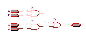
| + | == Circuito AND_NOR usando códigos sequenciais== | ||
| + | O circuito descrito abaixo somente executa o processo AND_GATES, quando uma das entradas (A, B, C ou D) é alterada. O mesmo ocorre em relação ao processo OR_GATE, que é executado quando uma das entradas I1 ou I2 é alterada. Finalmente o processo NOT_GATE é executado quando a entrada I3 é alterada. | ||
| + | |||
| + | Note que na primeira execução, todos os processos são executados uma vez, de modo a estabelecer valores iniciais válidos. Ou seja se todas entradas A, B, C, D estiverem em "0" => I1, I2, I3 = "0", => F = "1". Este valor é assumido após 2 ns no simulador. | ||
| + | |||
| + | <syntaxhighlight lang=vhdl> | ||
| + | entity and_or_not is | ||
| + | port | ||
| + | ( | ||
| + | A,B,C,D : in bit; | ||
| + | F : out bit | ||
); | ); | ||
| − | end | + | end and_or_not; |
| − | + | ||
| + | architecture v1 of and_or_not is | ||
| + | signal I1,I2,I3 : bit; | ||
| + | |||
begin | begin | ||
| − | + | AND_GATES: | |
| − | end | + | process(A, B, C, D) is |
| − | </ | + | begin |
| − | --> | + | I1 <= A and B after 2ns; |
| + | I2 <= C and D after 2ns; | ||
| + | end process; | ||
| + | |||
| + | OR_GATE: | ||
| + | process(I1, I2) is | ||
| + | begin | ||
| + | I3 <= I1 or I2 after 2ns; | ||
| + | end process; | ||
| + | |||
| + | NOT_GATE: | ||
| + | process(I3) is | ||
| + | begin | ||
| + | F <= not I3 after 2ns; | ||
| + | end process; | ||
| + | |||
| + | end v1; | ||
| + | |||
| + | </syntaxhighlight> | ||
| + | |||
| + | [[Imagem:and_nor.png|400px]] | ||
| + | |||
| + | Arquivo para teste em MODELSIM-ALTERA | ||
| + | <code> | ||
| + | vcom -93 -work work {/home/moecke/SST-2011-1/and_ou_not/and_ou_not.vhd} | ||
| + | vsim work.and_ou_not | ||
| + | |||
| + | add wave -divider {in} | ||
| + | add wave -color blue -format literal \ | ||
| + | {sim:/and_ou_not/a } \ | ||
| + | {sim:/and_ou_not/b } \ | ||
| + | {sim:/and_ou_not/c } \ | ||
| + | {sim:/and_ou_not/d } | ||
| + | |||
| + | add wave -divider {out} | ||
| + | add wave -color green -format literal\ | ||
| + | {sim:/and_ou_not/f } | ||
| + | |||
| + | add wave -divider {intern signals} | ||
| + | add wave -color yellow -format literal\ | ||
| + | {sim:/and_ou_not/i1 } \ | ||
| + | {sim:/and_ou_not/i2 } \ | ||
| + | {sim:/and_ou_not/i3 } | ||
| + | |||
| + | # Aguarda estabilizaçao inicial | ||
| + | run 3 ns | ||
| + | force -freeze sim:/and_ou_not/d 1 0 | ||
| + | run 8 ns | ||
| + | force -freeze sim:/and_ou_not/c 1 0 | ||
| + | run 8 ns | ||
| + | force -freeze sim:/and_ou_not/b 0 0 | ||
| + | run 8 ns | ||
| + | force -freeze sim:/and_ou_not/b 1 0 | ||
| + | run 8 ns | ||
| + | force -freeze sim:/and_ou_not/a 1 0 | ||
| + | run 8 ns | ||
| + | wave zoomfull | ||
| + | </syntaxhighlight> | ||
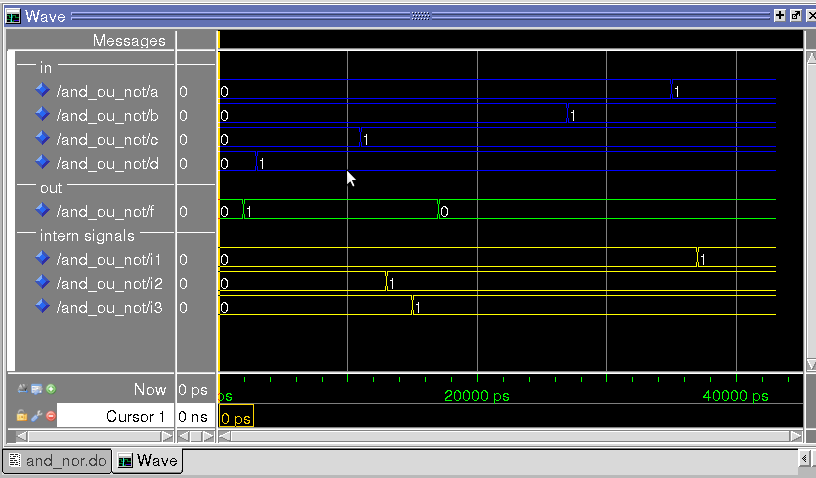
| + | Resultado do teste acima. | ||
| + | |||
| + | [[Imagem:and_nor_simul.png |600 px]] | ||
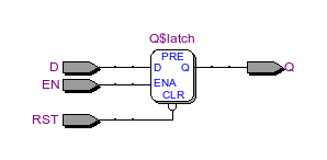
== Descrição do hardware de um Latch tipo D == | == Descrição do hardware de um Latch tipo D == | ||
O circuito descrito é ativo a entrada alto a entrada '''EN''' e ativo ao reset baixo '''RST''' | O circuito descrito é ativo a entrada alto a entrada '''EN''' e ativo ao reset baixo '''RST''' | ||
| − | <syntaxhighlight lang= | + | <syntaxhighlight lang=vhdl> |
library IEEE; | library IEEE; | ||
use IEEE.std_logic_1164.all; | use IEEE.std_logic_1164.all; | ||
| Linha 70: | Linha 225: | ||
</syntaxhighlight> | </syntaxhighlight> | ||
| − | [[Imagem:LATCHD.png]] | + | [[Imagem:LATCHD.png|400px]] |
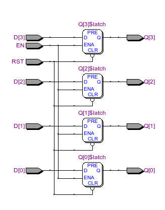
== Descrição do hardware de um registrador com 4 Latch tipo D == | == Descrição do hardware de um registrador com 4 Latch tipo D == | ||
O circuito descrito é ativo a entrada alto a entrada '''EN''' e ativo ao reset baixo '''RST''' | O circuito descrito é ativo a entrada alto a entrada '''EN''' e ativo ao reset baixo '''RST''' | ||
| − | <syntaxhighlight lang= | + | <syntaxhighlight lang=vhdl> |
library IEEE; | library IEEE; | ||
use IEEE.std_logic_1164.all; | use IEEE.std_logic_1164.all; | ||
| Linha 110: | Linha 265: | ||
Note neste exemplo o poder do VHDL de parametrizar o tamanho do registrador através do ''generic'' | Note neste exemplo o poder do VHDL de parametrizar o tamanho do registrador através do ''generic'' | ||
| − | <syntaxhighlight lang= | + | <syntaxhighlight lang=vhdl> |
library IEEE; | library IEEE; | ||
| Linha 139: | Linha 294: | ||
O circuito descrito é ativo a entrada de clk sensível a borda de subida | O circuito descrito é ativo a entrada de clk sensível a borda de subida | ||
| − | <syntaxhighlight lang= | + | <syntaxhighlight lang=vhdl> |
--------------------------------------- | --------------------------------------- | ||
LIBRARY ieee; | LIBRARY ieee; | ||
| Linha 173: | Linha 328: | ||
O circuito descrito é ativo a entrada de clk sensível a borda de subida | O circuito descrito é ativo a entrada de clk sensível a borda de subida | ||
| − | <syntaxhighlight lang= | + | <syntaxhighlight lang=vhdl> |
entity FFD is | entity FFD is | ||
| Linha 201: | Linha 356: | ||
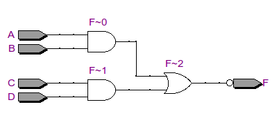
== Implementação de uma lógica combinacional And + Ou + Inversor (Direta) == | == Implementação de uma lógica combinacional And + Ou + Inversor (Direta) == | ||
| − | < | + | <syntaxhighlight lang=vhdl> |
library ieee; | library ieee; | ||
use ieee.std_logic_1164.all; | use ieee.std_logic_1164.all; | ||
| Linha 222: | Linha 377: | ||
[[Imagem:AOIv1.png]] | [[Imagem:AOIv1.png]] | ||
| − | < | + | <syntaxhighlight lang=vhdl> |
architecture v2 of AOI is | architecture v2 of AOI is | ||
signal I1, I2, I3 : std_logic; | signal I1, I2, I3 : std_logic; | ||
| Linha 237: | Linha 392: | ||
| − | < | + | <syntaxhighlight lang=vhdl> |
--------------------------------------- | --------------------------------------- | ||
LIBRARY ieee; | LIBRARY ieee; | ||
| Linha 271: | Linha 426: | ||
Faça um circuito que tenha duas entradas, sel (m bits) e ena (um bit), e uma saída x (n bits). Considere que n é potência binaria de dois, e m = log2 n. Se ena = '0', então todos os bits de x devem assumir o valor alto; caso contrário (ena = '1'), o bit correspondente ao valor indicado por sel deve ser '0' enquanto que os demais bits permanecem em '1'. Use o código abaixo como base para a generalização. | Faça um circuito que tenha duas entradas, sel (m bits) e ena (um bit), e uma saída x (n bits). Considere que n é potência binaria de dois, e m = log2 n. Se ena = '0', então todos os bits de x devem assumir o valor alto; caso contrário (ena = '1'), o bit correspondente ao valor indicado por sel deve ser '0' enquanto que os demais bits permanecem em '1'. Use o código abaixo como base para a generalização. | ||
| − | < | + | <syntaxhighlight lang=vhdl> |
--------------------------------------------- | --------------------------------------------- | ||
LIBRARY ieee; | LIBRARY ieee; | ||
| Linha 307: | Linha 462: | ||
</syntaxhighlight> | </syntaxhighlight> | ||
Para testar o DECODIFICADOR execute o código TCL do arquivo [[Media:Test_Dec3to8.txt| Test_Dec3to8.txt]] no Transcript-Window do ModelSim-Altera. | Para testar o DECODIFICADOR execute o código TCL do arquivo [[Media:Test_Dec3to8.txt| Test_Dec3to8.txt]] no Transcript-Window do ModelSim-Altera. | ||
| − | + | <syntaxhighlight lang=vhdl> | |
| + | do Test_Dec3to8.txt | ||
| + | </syntaxhighlight> | ||
| + | |||
| + | [[Categoria:VHDL]] | ||
Edição atual tal como às 17h13min de 18 de setembro de 2015
Descrição do hardware de uma porta E
entity PortaE is
	port
	(
		-- Input ports
		A,B	: in  bit;
		-- Output ports
		C	: out bit
	);
end entity PortaE;
architecture v1 of PortaE is


begin
 C <= A and B;
end architecture v1;
Descrição do hardware de um multiplexador de 4 para 1
entity mux_novo is
	port
	(
		-- Input ports
		X: in  bit_vector (3 downto 0);
                S : in bit_vector (1 downto 0);
		-- Output ports
		Y : out bit
	);
end entity mux_novo;

-- Implementação com lógica pura
architecture Logica_pura of mux_novo is

begin
 Y <= (X(0) and (not S(1)) and (not S(0))) or
      (X(1) and (not S(1)) and (S(0))) or
      (X(2) and (S(1)) and (not S(0))) or
      (X(3) and (S(1)) and (S(0)));
end architecture Logica_pura;

-- Implementação com WHEN ELSE
architecture v_WHEN of mux_novo is

begin
 Y <= X(0) when S = "00" else
      X(1) when S = "01" else
      X(2) when S = "10" else
      X(3);
end architecture v_WHEN;

-- Implementação com WITH SELECT
architecture v_WITH_SELECT of mux_novo is

begin
 with S select
 Y <= X(0) when "00",    -- note o uso da ,
      X(1) when "01",
      X(2) when "10",
      X(3) when others;  -- note o uso de others, para todos os demais valores.
                         -- Não pode ser substituido por "11" mesmo que o signal seja bit_vector.
end architecture v_WITH_SELECT;

-- Implementação com IF ELSE
architecture v_IF_ELSE of mux_novo is

begin


end architecture v_IF_ELSET;
vcom -93 -work work {/home/moecke/SST-2011-1/mux_41/mux_41.vhd}
vsim work.mux_41
add wave \
{sim:/mux_41/x } \
{sim:/mux_41/s } \
{sim:/mux_41/y }
- testando entrada 0
force -freeze sim:/mux_41/s 00 0
force -freeze sim:/mux_41/x 0001 0
run
force -freeze sim:/mux_41/x 1110 0
run
- testando entrada 1
force -freeze sim:/mux_41/s 01 0
force -freeze sim:/mux_41/x 0010 0
run
force -freeze sim:/mux_41/x 1101 0
run
- testando entrada 2
force -freeze sim:/mux_41/s 10 0
force -freeze sim:/mux_41/x 0100 0
run
force -freeze sim:/mux_41/x 1011 0
run
- testando entrada 3
force -freeze sim:/mux_41/s 11 0
force -freeze sim:/mux_41/x 1000 0
run
force -freeze sim:/mux_41/x 0111 0
run
</syntaxhighlight>
Circuito AND_NOR usando códigos sequenciais
O circuito descrito abaixo somente executa o processo AND_GATES, quando uma das entradas (A, B, C ou D) é alterada. O mesmo ocorre em relação ao processo OR_GATE, que é executado quando uma das entradas I1 ou I2 é alterada. Finalmente o processo NOT_GATE é executado quando a entrada I3 é alterada.
Note que na primeira execução, todos os processos são executados uma vez, de modo a estabelecer valores iniciais válidos. Ou seja se todas entradas A, B, C, D estiverem em "0" => I1, I2, I3  = "0", => F = "1".  Este valor é assumido após 2 ns no simulador.
entity and_or_not is
	port
	(
		A,B,C,D : in bit;
		F : out bit
	);
end and_or_not;


architecture v1 of and_or_not is

	signal I1,I2,I3 : bit;

begin
AND_GATES:
	process(A, B, C, D) is
	begin
		I1 <= A and B after 2ns;
		I2 <= C and D after 2ns;
	end process;

OR_GATE:
	process(I1, I2) is
	begin
		I3 <= I1 or I2 after 2ns;
	end process;

NOT_GATE:
	process(I3) is
	begin
		F <= not I3 after 2ns;
	end process;

end v1;
Arquivo para teste em MODELSIM-ALTERA

vcom -93 -work work {/home/moecke/SST-2011-1/and_ou_not/and_ou_not.vhd}
vsim work.and_ou_not
add wave -divider {in}
add wave -color blue -format literal \
{sim:/and_ou_not/a } \
{sim:/and_ou_not/b } \
{sim:/and_ou_not/c } \
{sim:/and_ou_not/d }
add wave -divider {out}
add wave -color green -format literal\

{sim:/and_ou_not/f }
add wave -divider {intern signals}
add wave -color yellow -format literal\
{sim:/and_ou_not/i1 } \
{sim:/and_ou_not/i2 } \
{sim:/and_ou_not/i3 }
- Aguarda estabilizaçao inicial
run 3 ns
force -freeze sim:/and_ou_not/d 1 0
run 8 ns
force -freeze sim:/and_ou_not/c 1 0
run 8 ns
force -freeze sim:/and_ou_not/b 0 0
run 8 ns
force -freeze sim:/and_ou_not/b 1 0
run 8 ns
force -freeze sim:/and_ou_not/a 1 0
run 8 ns
wave zoomfull
</syntaxhighlight>
Resultado do teste acima.

Descrição do hardware de um Latch tipo D
O circuito descrito é ativo a entrada alto a entrada EN e ativo ao reset baixo RST
library IEEE;
use IEEE.std_logic_1164.all;

entity LAD is
        port(
              D, EN, RST: in std_logic;
              Q: out std_logic
             );
end entity LAD;

architecture v1 of LAD is

begin

process (D,EN,RST)
begin
        if (RST = '0') then
                Q <= '0';       -- reset ocorre quando RST=0
        elsif (EN = '1') then
                Q <= D;         -- O valor de D passa para Q quando EN=1
        -- note que a falta do uso de um else indica que nada deve ser feito caso contrário,
        -- portanto o valor anterior de D permanece inalterado -> armazenamento (storage state)
        end if;
end process;

end architecture v1;

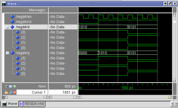
Descrição do hardware de um registrador com 4 Latch tipo D
O circuito descrito é ativo a entrada alto a entrada EN e ativo ao reset baixo RST
library IEEE;
use IEEE.std_logic_1164.all;

entity REGD4 is
 port(
      EN, RST: in std_logic;
      D: in std_logic_vector (3 downto 0);
      Q: out std_logic_vector (3 downto 0)
      );
end entity REG;

architecture v1 of REGD4 is

begin

process (D,EN,RST)
begin
   if (RST = '0') then
      Q <= "0000";  -- reset ocorre quando RST=0
   elsif (EN = '1') then
      Q <= D;  -- O valor de D passa para Q quando EN=1
   end if
end process;

end architecture v1;


Descrição do hardware de um registrador com N Latch tipo D
O circuito descrito é ativo a entrada alto a entrada EN e ativo ao reset baixo RST
Note neste exemplo o poder do VHDL de parametrizar o tamanho do registrador através do generic
library IEEE;
use IEEE.std_logic_1164.all;

entity REGDN is
 generic (N: integer := 4)
 port(EN, RST: in std_logic;
  D: in std_logic_vector (N-1 downto 0);
  Q: out std_logic_vector (N-1 downto 0));
end entity REGDN ;

architecture v2 of REGDN is
begin
process (D,EN,RST)
begin
 if (RST = '0') then
  Q <= (others =>  '0'); -- reset todos os bits Q quando RST=0
 elsif (EN = '1') then
  Q <= D;  -- passa todos os valores de D para as saídas Q correspondentes
 end if;
end process;
end architecture v2;
Descrição do hardware de um Flip Flop tipo D
O circuito descrito é ativo a entrada de clk sensível a borda de subida
---------------------------------------
LIBRARY ieee;
USE ieee.std_logic_1164.all;
---------------------------------------
ENTITY DFF IS
PORT
   (
   d, clk, rst: IN STD_LOGIC;
   q: OUT STD_LOGIC
	);
END DFF;
---------------------------------------
ARCHITECTURE behavior OF DFF IS

BEGIN
PROCESS (rst, clk)
BEGIN
    IF (rst='1') THEN
	    q <= '0';
    ELSIF (clk'EVENT AND clk='1') THEN
       q <= d;
    END IF;

END PROCESS;
END behavior;
---------------------------------------
Implementação de uma lógica combinacional And + Ou + Inversor (Direta)
library ieee;
use ieee.std_logic_1164.all;

entity AOI is
	port
	(
		A,B, C, D	: in  std_logic;
		F	: out std_logic
	);
end AOI;

architecture v1 of AOI is
begin
	F <= not((A and B) or (C and D));
end v1;

architecture v2 of AOI is
   signal I1, I2, I3 : std_logic;
begin
   I1 <= A and B;
   I2 <= C and D;
   I3 <= I1 or I2;
   F <= not I3;
end v2;
Problema 2.1: Multiplexer
Faça um multiplexador que selecione a entrada A para sel ='01', B para sel ='10', coloque '0...0' na saída para sel ='00'e mantenha a saída em alta impedância "Z...Z" quando sel='11'.
---------------------------------------
LIBRARY ieee;
USE _________________________ ;
---------------------------------------
ENTITY mux IS
PORT ( __ , __ : ___ STD_LOGIC_VECTOR (7 DOWNTO 0);
sel : IN ____________________________ ;
___ : OUT STD_LOGIC_VECTOR (7 DOWNTO 0));
END _____ ;
---------------------------------------
ARCHITECTURE example OF _____ IS
BEGIN
PROCESS (a, b, ____ )
BEGIN
IF (sel = "00") THEN
c <= "00000000";
ELSIF (__________) THEN
c <= a;
_____ (sel = "10") THEN
c <= __;
ELSE
c <= (OTHERS => '__');
END ___ ;
END _________ ;
END _________ ;
---------------------------------------
Problema 4.1: Decodificador Genérico - ativo baixo
Faça um circuito que tenha duas entradas, sel (m bits) e ena (um bit), e uma saída x (n bits). Considere que n é potência binaria de dois, e m = log2 n. Se ena = '0', então todos os bits de x devem assumir o valor alto; caso contrário (ena = '1'), o bit correspondente ao valor indicado por sel deve ser '0' enquanto que os demais bits permanecem em '1'. Use o código abaixo como base para a generalização.
---------------------------------------------
LIBRARY ieee;
USE ieee.std_logic_1164.all;
---------------------------------------------
ENTITY decoder IS
	PORT (
		ena : IN STD_LOGIC;
		sel : IN STD_LOGIC_VECTOR (2 DOWNTO 0);
		x : OUT STD_LOGIC_VECTOR (7 DOWNTO 0));
END decoder;
---------------------------------------------
ARCHITECTURE generic_decoder OF decoder IS
BEGIN
PROCESS (ena, sel)
	VARIABLE temp1 : STD_LOGIC_VECTOR (x'HIGH DOWNTO 0);
	VARIABLE temp2 : INTEGER RANGE 0 TO x'HIGH;       -- Poderia também usar x'REVERSE_RANGE
BEGIN
	temp1 := (OTHERS => '1');
	temp2 := 0;
	IF (ena='1') THEN
		FOR i IN sel'RANGE LOOP      -- Forma genérica de definir o "RANGE 2 downto 0"
			IF (sel(i)='1') THEN -- Conversão de Binário para Decimal
				temp2:=2*temp2+1;
			ELSE
				temp2 := 2*temp2;
			END IF;
		END LOOP;
		temp1(temp2):='0';
	END IF;
	x <= temp1;
END PROCESS;
END generic_decoder;
---------------------------------------------
Para testar o DECODIFICADOR execute o código TCL do arquivo Test_Dec3to8.txt no Transcript-Window do ModelSim-Altera.
do Test_Dec3to8.txt